Semiconductors are the brains of modern electronics, tiny chips that make everything from smartphones to self-driving cars possible. But the path from raw materials to a finished microchip is one of the most complex and precise manufacturing journeys in the world.
This post walks through that journey, explaining the major stages chipmakers use to fabricate powerful, reliable semiconductor devices. For broader industry context, organizations like SME and NIST MEP provide additional insight into advanced manufacturing practices.
Silicon wafer creation: the blank canvas
The semiconductor manufacturing process begins long before circuits are formed. It starts with the creation of the material foundation that every chip relies on.
From sand to polished wafer
Manufacturers start with ultra-pure silicon, typically derived from sand. They melt the silicon and form it into a cylindrical crystal called an ingot, then slice the ingot into wafer-thin discs and polish each one to a mirror-smooth finish.
These wafers will become the blank canvas for building circuits. Precision at this stage is crucial, since even microscopic imperfections can lead to defects later.
This emphasis on starting material quality mirrors broader manufacturing guidance highlighted by NIST MEP, where upstream control directly affects downstream yield.
Front-end fabrication: building circuits on the wafer
Front-end fabrication is where the most intricate work of semiconductor manufacturing takes place. This stage involves repeating a series of tightly controlled steps inside ultra-clean fabrication facilities to create circuits on the wafer.
Thin-film deposition
Manufacturers deposit thin layers of conducting, semiconducting, or insulating material onto the wafer surface. They use techniques such as chemical vapor deposition and physical vapor deposition to lay down the foundational layers that later form transistors and interconnects.
These layers must be uniform at the atomic level to ensure consistent electrical performance across the wafer.
Photolithography
Photolithography functions like micro-scale printing. A light-sensitive chemical called photoresist is applied to the wafer, and ultraviolet light shines through a patterned mask to transfer the circuit design onto the surface.
Advanced facilities may use extreme ultraviolet lithography to define features that are only a few nanometers wide.
Etching
After lithography, manufacturers selectively etch the wafer to remove unwanted material and expose the intended circuit patterns. They perform etching using either wet chemical processes or dry, plasma-based techniques.
The choice depends on the material being removed and the level of precision required.
Ion implantation and doping
To control how electrons move through silicon, manufacturers introduce precise amounts of dopant atoms such as boron or phosphorus. This process alters the electrical characteristics of specific regions on the wafer.
Doping is essential for forming transistors and enabling the on and off switching behavior that defines digital logic.
Planarization and cleaning
As multiple layers accumulate, surfaces must be flattened using chemical-mechanical polishing so that additional layers can be added without distortion.
Throughout fabrication, manufacturers repeatedly clean wafers to remove microscopic contaminants that could compromise circuit performance. They follow cleanroom discipline that aligns with manufacturing safety and contamination-control principles outlined by OSHA.
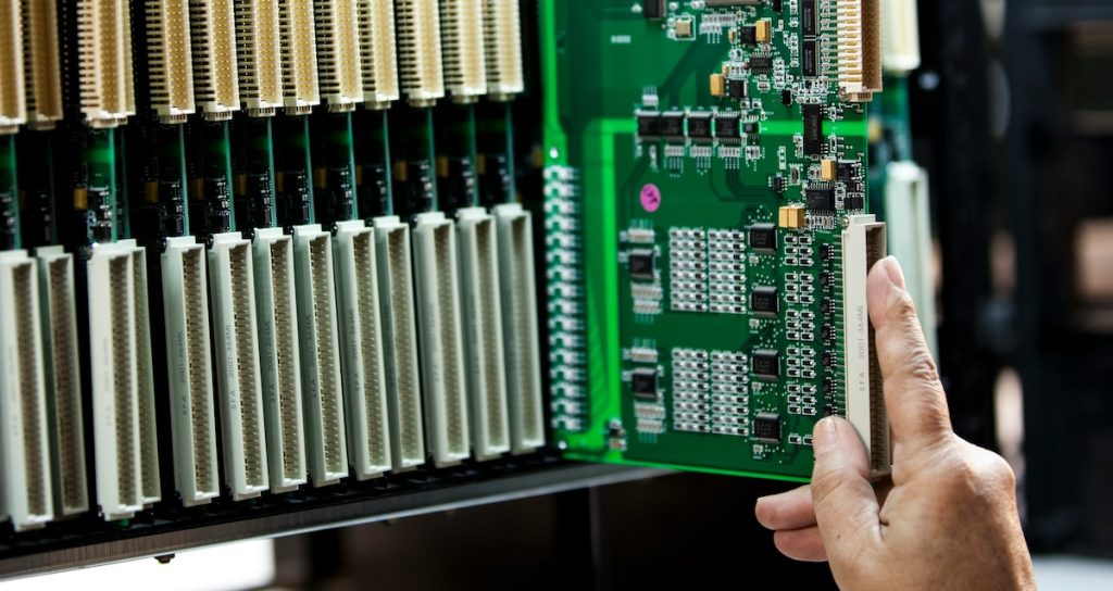
Back-end processing: turning wafers into chips
Once all circuit layers are complete, the wafer moves into back-end processing. This phase converts a finished wafer into individual, usable semiconductor devices.
Wafer dicing
The wafer is cut into individual dies using precision saws or laser systems. This step, often called die singulation, separates each functional circuit from the wafer.
Manufacturers handle the wafers with extreme care to avoid damaging the delicate structures formed during front-end fabrication.
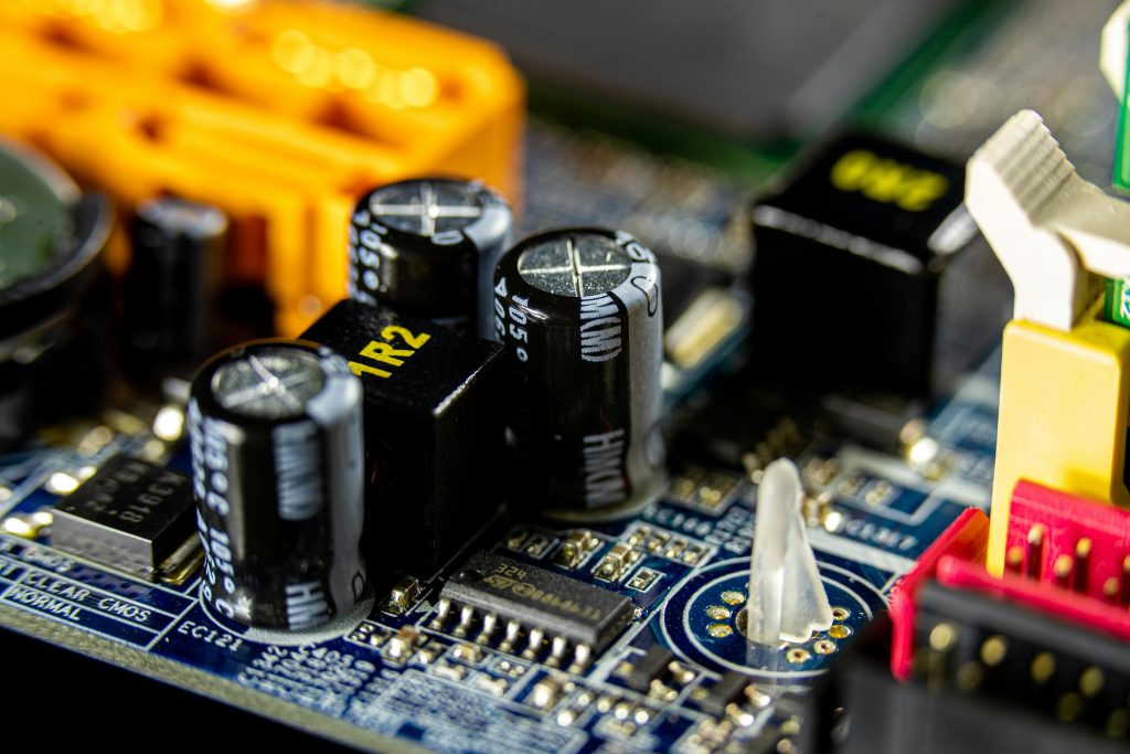
Packaging and electrical connection
Manufacturers mount each die into a protective package that shields it from physical damage and environmental exposure, then create electrical connections using wire bonding or flip-chip techniques.
The package allows the chip to interface reliably with circuit boards and external systems.
Testing and quality control
Before shipment, manufacturers test every chip extensively to verify functionality, speed, and reliability, and they reject any devices that fail to meet specifications.
Additional inspections check for physical defects that may not immediately affect performance but could shorten lifespan.
Why semiconductor manufacturing is so challenging
Semiconductor fabrication demands an extraordinary level of control, coordination, and precision across every stage of production.
Extreme cleanroom requirements
Fabrication takes place in cleanrooms that are far cleaner than hospital operating rooms. Even a single dust particle can render a chip unusable.
Nanometer-scale precision
Modern chips contain billions of transistors, with features measured in single-digit nanometers. This requires precise control of light, chemicals, temperature, and motion.
Continuous process feedback
Front-end and back-end manufacturing teams constantly share data to identify defects, improve yields, and refine process steps.
This continuous feedback loop is essential for maintaining performance and reliability at scale, a theme commonly discussed in advanced manufacturing research from institutions like MIT Sloan.
How precision manufacturing supports chip production
Chipmakers rely on components and systems with micron-level tolerances to maintain performance and yield. Precision machining and fabrication play a critical role in supporting the tools and equipment used in fabs.
Supporting equipment and infrastructure
From CNC-machined parts for wafer handling systems to cleanroom-compatible sheet metal assemblies, each precision part helps keep production running smoothly.
Powerful, compact chips
From raw silicon to finished microchip, semiconductor manufacturing combines physics, chemistry, materials science, and precision engineering.
Every stage, from wafer creation through repeated lithography, etching, doping, and packaging, plays a critical role.
The result is the powerful, compact chips that drive modern technology across industries and everyday life.
FAQ
People most often ask these questions when they learn how semiconductor chips are made.
What materials are used to make semiconductor chips?
Manufacturers make most semiconductor chips from silicon because it is abundant, stable, and delivers ideal electrical properties. They add small amounts of dopants such as boron or phosphorus to precisely control how electricity flows through the chip.
Why does semiconductor manufacturing require cleanrooms?
Chip features are measured at the nanometer scale, so even microscopic dust particles can damage circuits. Cleanrooms control airborne particles, temperature, humidity, and vibration to protect wafers during fabrication.
How long does it take to manufacture a semiconductor chip?
From raw silicon to a finished packaged chip, the manufacturing process can take several weeks to months, depending on complexity and testing requirements.
What is the difference between front-end and back-end fabrication?
Front-end fabrication focuses on building transistors and circuits directly on the silicon wafer, while back-end processing involves cutting the wafer into individual chips, packaging them, and performing final testing.
Why are semiconductor chips so expensive to produce?
Chip manufacturing requires advanced equipment, extreme precision, and highly controlled environments. Facility costs, tooling, and ongoing process development contribute significantly to overall cost.