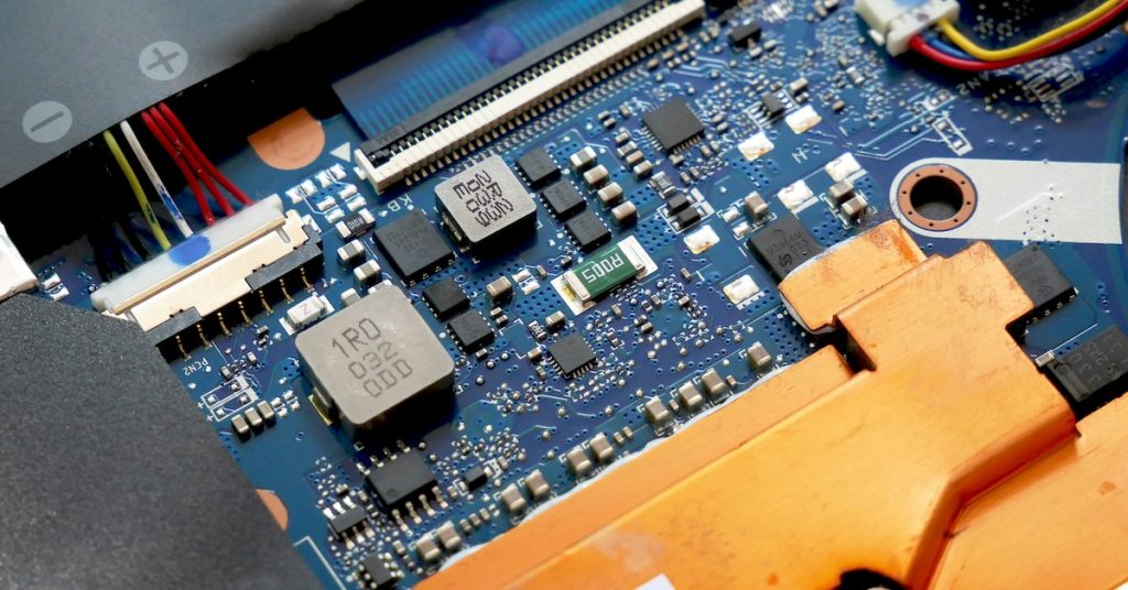
From smartphones and electric vehicles to aerospace systems and medical devices, semiconductors power nearly every piece of modern technology. These tiny chips, often smaller than a fingernail, enable high-speed computing, data processing, and intelligent automation.
But behind each chip lies an incredibly complex, precision-driven process: semiconductor manufacturing.
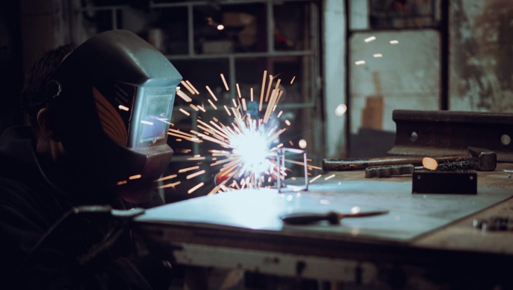
At Eagle Metalcraft, we understand the critical role high-performance components play in this field. As a trusted partner to companies across the electronics and semiconductor supply chain, we support this fast-moving industry with precision sheet metal parts, CNC-machined enclosures, cleanroom-ready components, and more.
What Are Semiconductors?
Semiconductors are materials with electrical conductivity between that of conductors and insulators. Silicon is the most commonly used, though materials like gallium arsenide and silicon carbide are also used in high-performance applications.
How Semiconductor Materials Function
When engineered into chips, semiconductors can control electrical signals, store data, and execute complex instructions. These microdevices form the heart of everything from smartphones to satellites.
Engineering resources from ASME frequently explore the materials science and engineering principles behind semiconductor technologies.
Key Steps in the Semiconductor Manufacturing Process
The path from raw silicon to finished chip is intricate and exacting. Multiple stages transform purified materials into microscopic circuits capable of performing billions of operations per second.
Wafer Fabrication
Semiconductor devices begin as thin silicon wafers, sliced from purified crystal ingots. These wafers are polished to a mirror finish and prepared for circuitry.
Manufacturing resources from The Fabricator frequently examine precision processes used in advanced manufacturing environments.
Photolithography
A light-sensitive photoresist is applied to the wafer surface. Ultraviolet light transfers a circuit pattern onto the wafer, creating microscopic pathways for current.
Manufacturing research from NIST MEP highlights how process control and precision engineering support consistency in advanced manufacturing.
Etching and Doping
Unwanted material is chemically etched away, and selected areas are doped with ions to alter electrical properties. This forms the foundation of each transistor and integrated circuit.
Industry organizations such as SME regularly discuss manufacturing technologies and process optimization used in advanced electronics production.
Deposition and Metallization
Thin layers of insulating and conductive materials coat the wafer. Metal traces follow, connecting circuit elements to form working chips.
Assembly and Packaging
Manufacturers test the finished chips, separate them from the wafer, and package them in protective casings for integration into electronic devices.
Industry analysis from McKinsey Manufacturing Insights often examines semiconductor supply chains and the complexity of modern chip production.
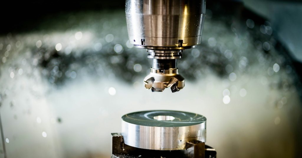
How Precision Manufacturing Supports Semiconductor Success
Because the features on a semiconductor can be smaller than 10 nanometers, manufacturing requires extraordinary accuracy and consistency. Precision machining, cleanroom environments, and advanced automation all play a role in meeting these demands.
Where Eagle Metalcraft Adds Value
Semiconductor manufacturing demands extreme precision, clean environments, and exacting tolerances. That’s where Eagle Metalcraft adds value, supporting equipment builders that follow global manufacturing standards.
- CNC-machined parts for wafer handling systems and enclosures
- Sheet metal fabrication for cleanroom frames, cabinets, and structural components
- Stainless steel and anodized aluminum parts suitable for contamination-sensitive environments
- Custom fixturing, tooling, and one-off prototyping for research and development applications
International standards organizations such as ISO provide widely referenced manufacturing and quality management frameworks used across advanced industries.
Common Challenges in Semiconductor Manufacturing
Semiconductor fabrication is one of the most technically demanding manufacturing processes in the world. Chipmakers must balance extreme precision with high-volume production and global supply chain complexity.
Miniaturization
Modern chips feature elements measured in nanometers. This scale demands advanced lithography techniques and microscopic precision across every step of the manufacturing process.
Supply Chain Risk
Geopolitical shifts and global disruptions have led to increased focus on domestic production and localized supplier networks.
Research from Deloitte Manufacturing Insights frequently analyzes semiconductor supply chain resilience and reshoring strategies.
Thermal and Electrical Demands
New applications like electric vehicles and high-speed communications require semiconductors capable of operating under higher voltages and temperatures. These requirements drive the need for stronger materials and tighter tolerances.
Cleanroom Compatibility
Manufacturers must eliminate dust, oils, and static during production. Precision parts must be designed and finished to withstand strict contamination controls.
Workplace safety guidance from OSHA outlines safety and environmental practices relevant to advanced manufacturing facilities.
Trends Reshaping the Semiconductor Industry
As demand continues to grow and applications expand, the semiconductor industry is evolving rapidly. New technologies and manufacturing strategies are transforming chip production.
Smart Manufacturing
Connected machines, predictive maintenance, and real-time process data are turning semiconductor fabrication facilities into highly optimized smart factories.
Research published by MIT Sloan frequently explores digital transformation and smart manufacturing strategies.
Advanced Materials
Manufacturers increasingly rely on advanced alloys, ceramics, and composites for next-generation chip production tools and packaging.
Materials standards and testing frameworks are frequently developed and maintained by ASTM International.
Automation
Robotic wafer handling and AI-driven inspection systems are improving production speed, repeatability, and yield.
Manufacturing education and research from SME often highlight automation as a critical driver of modern industrial productivity.
Sustainability Focus
Manufacturers are seeking energy-efficient processes, reduced material waste, and environmentally responsible supply chains as semiconductor production scales globally.
FAQ
Semiconductor manufacturing remains one of the most advanced and precise processes in modern industry. From everyday consumer electronics to advanced transportation and aerospace systems, semiconductors enable modern digital technology.
What is a semiconductor?
A semiconductor is a material with electrical conductivity between that of a conductor and an insulator. Silicon is the most commonly used semiconductor material.
How are semiconductors used in everyday technology?
Semiconductors power computers, smartphones, vehicles, medical equipment, household appliances, and industrial control systems.
What is semiconductor manufacturing?
Semiconductor manufacturing is the process of transforming raw semiconductor materials into functional microchips through steps such as wafer fabrication, photolithography, etching, and packaging.
Why are cleanrooms important?
Cleanrooms control airborne particles, humidity, and static to prevent contamination. Even microscopic particles can damage semiconductor devices during fabrication.
How precise is semiconductor manufacturing?
Modern semiconductor manufacturing operates at nanometer-scale precision and relies on advanced process control, specialized materials, and extremely controlled production environments.